What is impurity ion scattering? How is it impacted by dopant concentration and temperature?
答案 点击查看
Impurity ion scattering is the deflection(偏转) of mobile charge carriers (electrons or holes) by the fixed, ionized impurity atoms in a semiconductor.
Dopant Concentration: A higher concentration of dopant ions creates more scattering sites, which significantly increase Impurity Scattering and decreases carrier mobility.
Temperature: This scattering effect is strong at low temperatures and becomes weaker as temperature increases, because carriers with higher thermal energy are less easily deflected.
Phonon scattering is the collision (碰撞) of mobile charge carriers with the vibrating crystal lattice(振动的晶格), or equivalently with phonons, the quantized particles that carry lattice-vibration energy (声子是晶格振动能量的量子).
Temperature: As temperature increases, lattice vibrations become stronger and the phonon density rises, leading to more frequent carrier–phonon collisions. This increases phonon scattering and reduces mobility; roughly, the phonon-limited mobility scales as μphonon∝T(−3/2), so higher T → lower μ.
Charge–charge scattering (载流子–载流子散射) is the deflection (偏转) of a mobile charge carrier by the Coulomb force from other mobile carriers (electron–electron or electron–hole interactions).
Carrier Concentration: It is only significant at high carrier concentrations, where many carriers are present and the probability of carrier–carrier Coulomb interactions becomes large, thus reducing mobility.
Temperature: With increasing temperature, carriers move faster, so their interaction time with any given charged neighbor is shorter and the Coulomb deflection angle becomes smaller. Therefore charge–charge scattering becomes weaker as temperature rises, and its impact on mobility decreases.
Net Current: In the absence of an electric field or concentration/temperature gradients, carriers undergo only random thermal motion; the average current in any direction is zero. Directed current requires a driving force (electric field for drift, or concentration/temperature gradients for diffusion), while scattering mainly limits how large this directed motion (mobility, diffusivity) can become.
What is the “effective mass of electron” in a semiconductor? List two factors that may have influence on its value.
答案 点击查看
The effective mass (m∗) is the mass parameter that makes an electron in a periodic crystal respond to forces(在周期性晶格势场中对于外界力量的质量参数) (electric, magnetic) as if it were a free particle.
It is influenced by:
The Material: Its value is determined by the material's unique electronic band structure.
Crystal Direction: Different crystal directions have different band curvature (能带弯曲)→ different m∗.
Strain: Changes lattice spacing/symmetry(改变晶格间距/对称性), reshaping band curvature (dk2d2E) → different m∗.
Lower the lattice temperature to suppress(抑制) phonon scattering (phonon density↓, mobility↑).
Use Strain Engineering: Straining the crystal lattice (e.g. strained silicon) can alter the band structure to reduce effective mass, thereby improving mobility
Impact on Device Performance:
Higher carrier mobility directly results in higher current drive (I∝μ) and lower resistance. This allows transistors to switch faster, leading to higher operating frequencies (fT) and improved overall device speed.
What is the concept of “velocity saturation” in a semiconductor? How does it impact an electronic device's behavior?
答案 点击查看
When the kinetic energy(动能) of a carrier exceeds a critical value(达到某个临界值), it generates an optical phonon(光学声子) and loses the kinetic energy. Therefore, the kinetic energy is capped at large E, and the velocity does not rise above a saturation velocity, vsat
In short-channel transistors, this effect is what causes the drain current to saturate, limiting the maximum current and switching speed.
Regarding carrier movement in semiconductor, what is the difference between thermal velocity and drift velocity?
答案 点击查看
Thermal velocity is the random motion(随机) of carriers in all directions due to thermal energy, while drift velocity is the small average velocity (很小的平均漂移速度) superimposed(叠加) on this random motion when an electric field is applied.
Thermal velocity depends on temperature and effective mass Vth=mn∗3kT. But drift velocity depends on the electric field's value , meaning free time and effective mass ∣Vd∣=mn∗qEτmin.
What is the carrier generation process in semiconductors? List three possible mechanisms for this process.
答案 点击查看
Carrier generation is the process that creates electron–hole pairs in a semiconductor by exciting electrons from the valence band to the conduction band (possibly via defect levels可能经过缺陷能级).
Three possible mechanisms
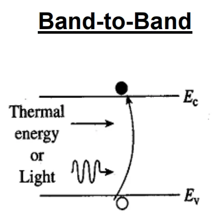
Band-to-Band Generation(带-带产生)Thermal energy or photons with energy≥Eg directly excite an electron from the valence band Ev to the conduction band Ec, creating an electron–hole pair.
Thermal: energy comes from lattice vibrations (heat/phonons).
Optical (photogeneration): energy comes from absorbed photons(注意这是photon不是phonon).
然后可以画个图:
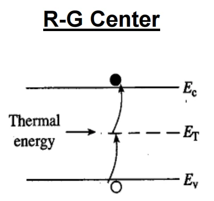
R-G Center Generation(通过 R-G 中心产生)Recombination–generation (R-G) centers are defect(缺陷)/impurity(杂质)/surface states(表面态) that introduce an energy levelETinside the bandgap. With thermal energy, carriers are generated in two steps via this level (e.g. Ev→ET→Ec), producing an electron–hole pair.
R-G centers are a major source of thermal generation and of reverse saturation current in devices.
Impact Ionization(碰撞电离)
In a strong electric field, carriers are accelerated and gain high kinetic energy between collisions. A “hot” carrier can collide with the lattice and knock an electron from the valence band to the conduction band, creating a new electron–hole pair.
This is the basic mechanism behind avalanche multiplication and avalanche breakdown.
提醒
原答案
Carrier generation is the process that creates electron-hole pairs in a semiconductor, where an electron is excited from the valence band to the conduction band.
Thermal Generation: Energy from lattice vibrations (heat/phonons) excites an electron across the band gap.
Optical Generation (Photogeneration): A photon with energy greater than the band gap is absorbed, creating an electron.
Impact Ionization: A high-energy carrier collides with the lattice and uses its kinetic energy to excite a new electron-hole pair.
Electric field: The field makes the energy gap thin,so that the electrons can be more easily excited.
In a pn junction, what conditions must be met (in terms of carrier concentrations) so that (a) the n-side, and (b) the p-side can be considered as “low-level injection”, respectively?
答案 点击查看
On the n-side (n-type region):
The injected excess hole concentration(注入过剩空穴浓度) is much smaller than the equilibrium majority electron concentration:
so the total electron concentration is essentially unchanged, nn≈nn0.
On the p-side (p-type region):
The injected excess electron concentration is much smaller than the equilibrium majority hole concentration:
so the total hole concentration is essentially unchanged, pp≈pp0
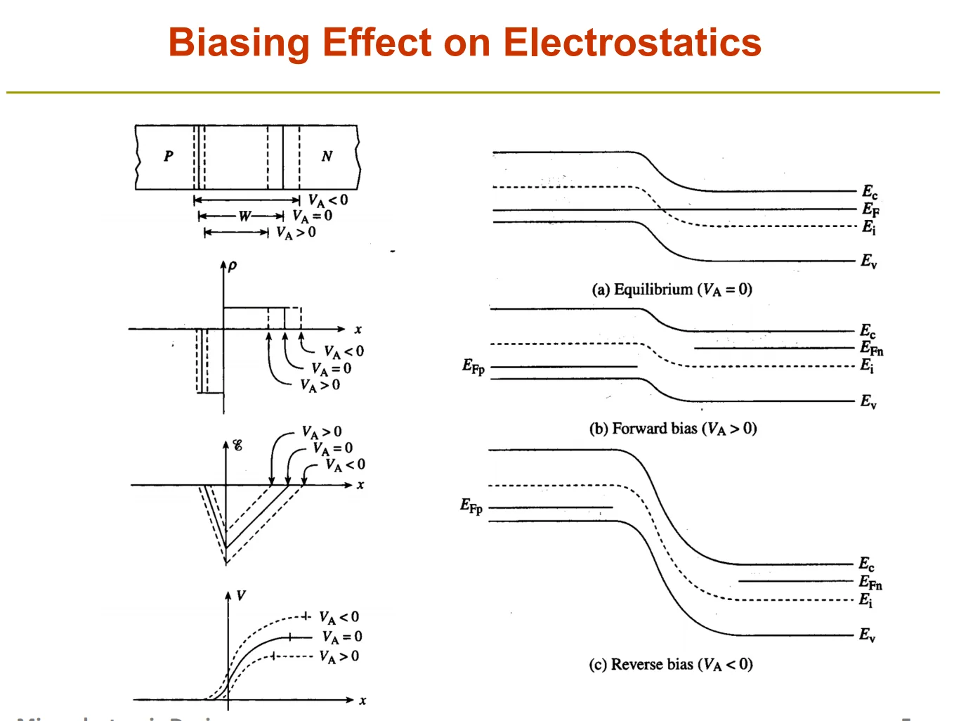
What is the meaning of “quasi Fermi level” in a semiconductor? Schematically (示意性地) draw the band diagram of a p+n junction in (a) forward-biased and (b) reverse-biased p+n junction, respectively. In your plot, show Ec, EFn, EFp, Ei and Ev, respectively.
答案 点击查看
Quasi-Fermi levels are separate effective Fermi levels for electrons and holes used when a semiconductor is out of thermal equilibrium. They are defined so that the carrier concentrations can still be written as

评论区