PN Junction
PN Junction Fabricate
将P型杂质扩散到均匀掺杂的N型衬底
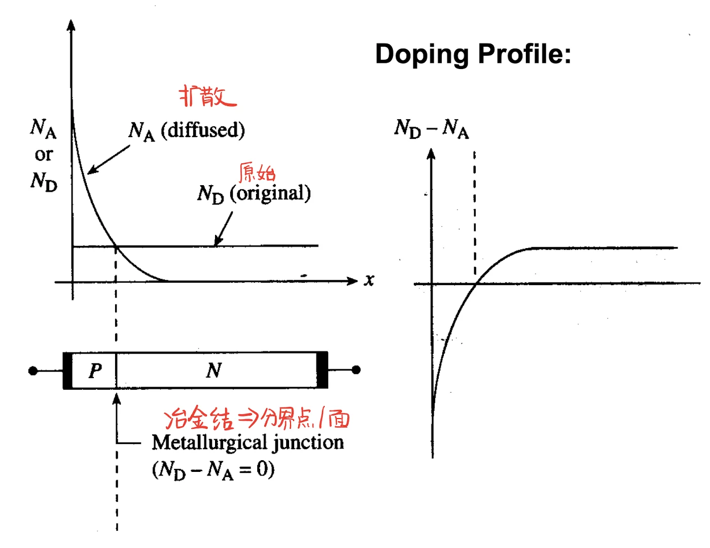
Ideal PN Junction | 理想PN结
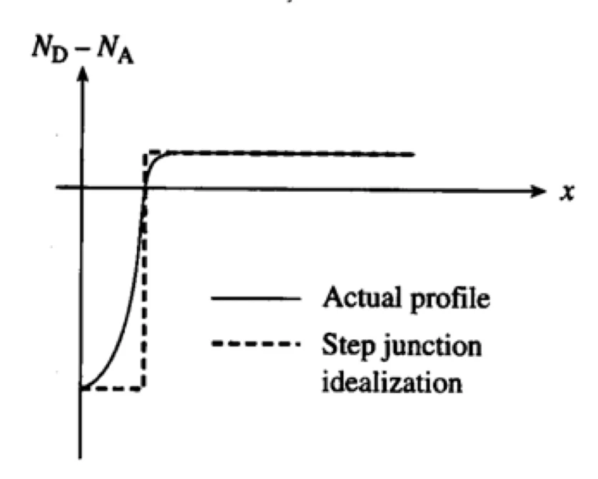
Step (Abrupt) Junctions | 陡变结
分布近似于虚线所示
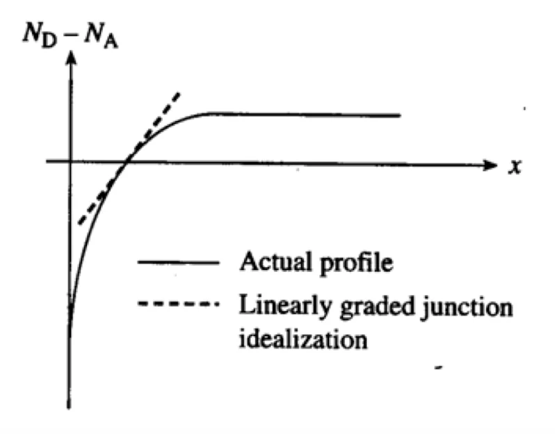
Graded (Linear) Junction | 线性结
Electrical Characteristics | 电学特性
Charge Density in a Semiconductor | 电荷密度
Assuming the dopants are completely ionized,then the net charge density is:
事实上静电荷数密度是 (p+ND)−(n+NA)
Gauss's Law & Poission's Equation
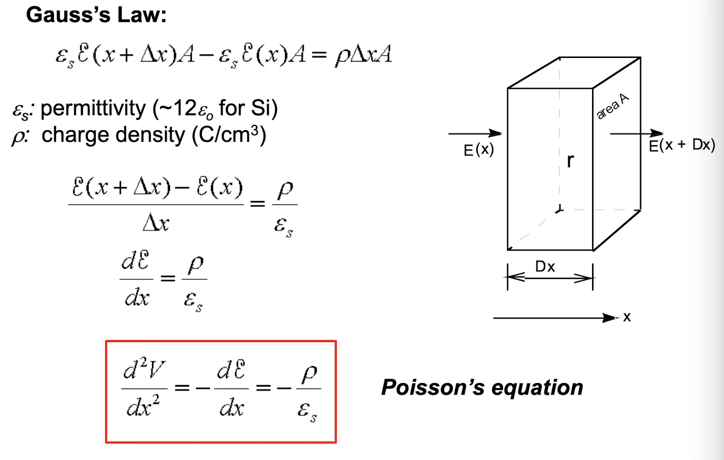
这里注意 ,以及高斯定理和泊松方程
Energy Band Diagram | 能带图
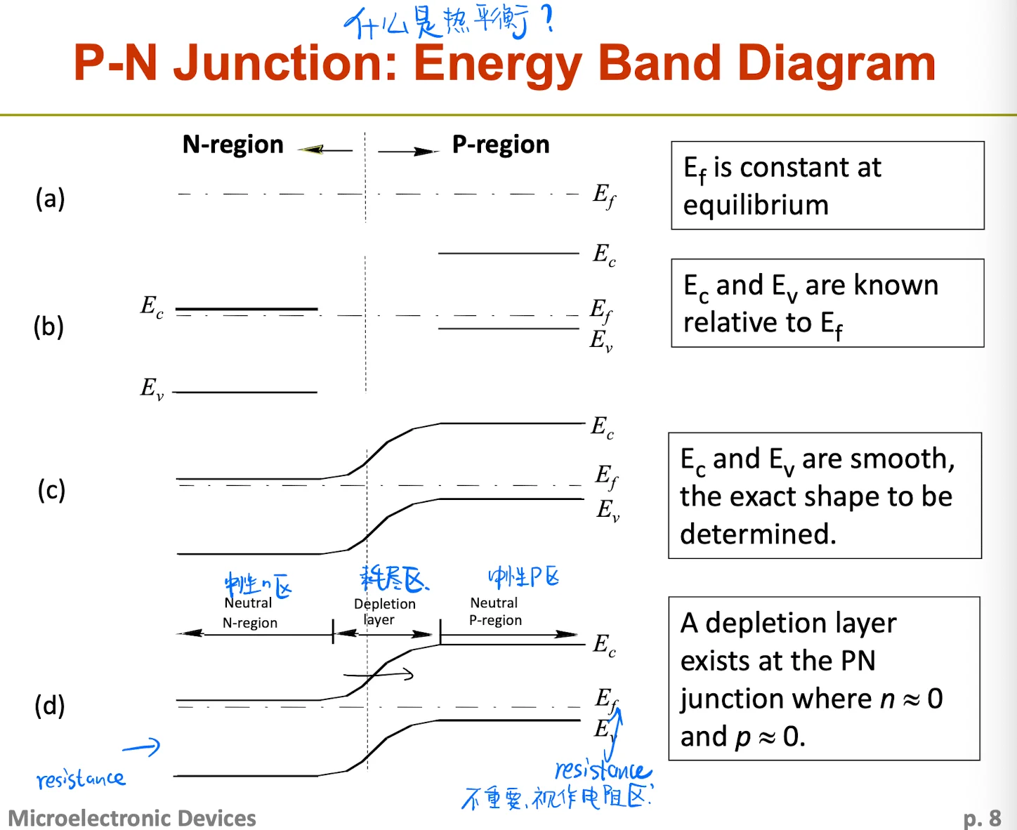
- Ef is constant at equilibrium and Ec,Ev are known relative to Ef
热平衡时费米能级 必须是常数
,由玻尔兹曼近似就可以算出不同位置x的电子or空穴浓度
所以哪边 更低(更靠近 )哪边就更 n 型;哪边 更高哪边就更 p 型
- Ec and Ev are smooth , the exact shape to be determined
- A depletion lay exists at the PN junction where n≈0 and p≈0
The built-in potential is generated due to band bending.
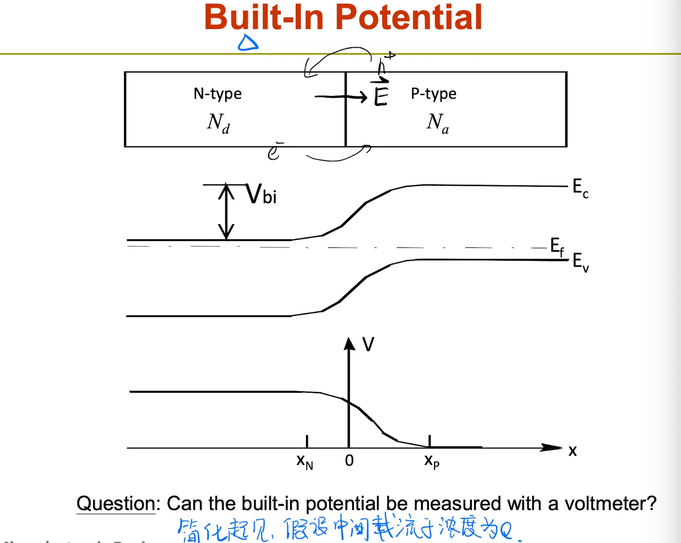
Question: Can the built-in potential be measured with a voltmeter?
不可以。使用一个标准的电压表直接测量PN结的内建电势 (Vbi),读数将为0伏特。
- 产生新的接触电势 当电压表的金属探针接触P型区和N型区时,会在“金属-P型”和“金属-N型”的界面上形成两个新的接触电势 (Contact Potentials)。
- 热平衡抵消
电压表、探针和PN结形成一个完整的闭合回路。在热平衡状态下(无电流流过),此回路中所有电势差的总和必须为零。
- 其中 就是内建电势 。
- 物理规律决定了新产生的两个接触电势(V金属-P 和 VN-金属)与内建电势 Vbi 恰好完全相互抵消。
- 费米能级解释 电压表测量的是其两探针之间的费米能级 (EF) 之差。在热平衡状态下,整个闭合回路的费米能级处处相等(为一条平线)。因此,两探针间的费米能级之差为零,电压表读数即为零。
只能通过间接方法(如C-V电容-电压特性测量法)来推算得出。
Quantitative Analysis | 定量分析
Depletion Approximation
Depletion approximation | 耗尽区近似
a. 耗尽区内没有可移动的电子和空穴;b. 耗尽区外假设为中性,净电荷浓度为0;
- Inside the Depletion Region: It assumes there are no mobile electrons or holes (n=0, p=0). The charge consists only of fixed donor () and acceptor () ions.
- Outside the Depletion Region (Neutral Region): It assumes the region is perfectly neutral, meaning the net charge density is zero ().
Built-in Potential
Non-degenerately doped | 非简并掺杂
指半导体中中等或轻度的掺杂水平,掺杂浓度不足以使费米能级 () 进入导带 () 或价带 ()。费米能级始终位于禁带之内。
Refers to a moderate or light doping level in semiconductors, where the doping concentration is not sufficient to shift the Fermi level () into the conduction band () or the valence band (). The Fermi level remains within the band gap at all times.
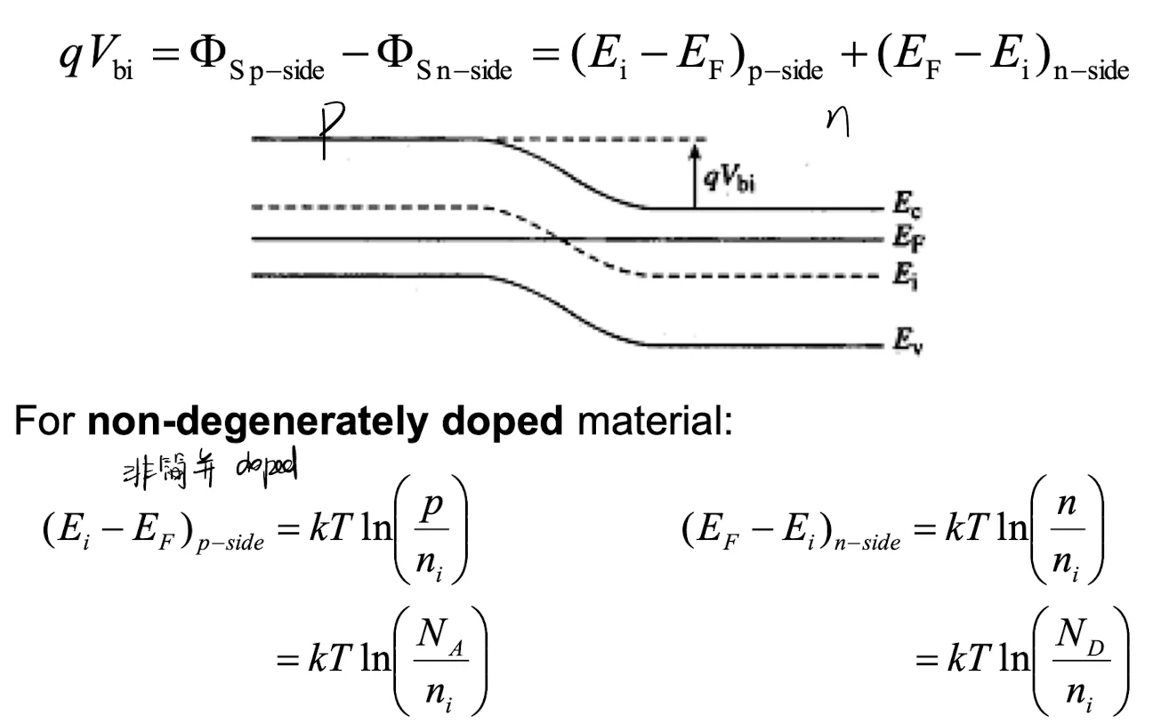
Then we can get the value of (前提是非简并材料 non-degenerately doped):
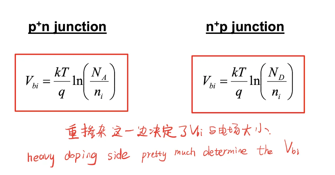
for Abrupt PN Junctions
The heavy doping side pretty much determine the | 重掺杂这一边决定了 和电场的大小
Calculation of E(x) V(x)
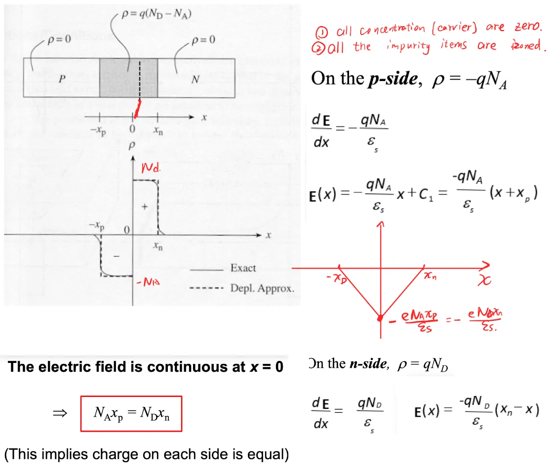
The electric field is continuous at x= 0
电场是连续不光滑函数,电势是连续且光滑的函数
对电场进行积分可以得到(此处令 作为0电势参考点)
- On the P side:
- On the N side :
也可以得到同时有
得到如下一系列公式
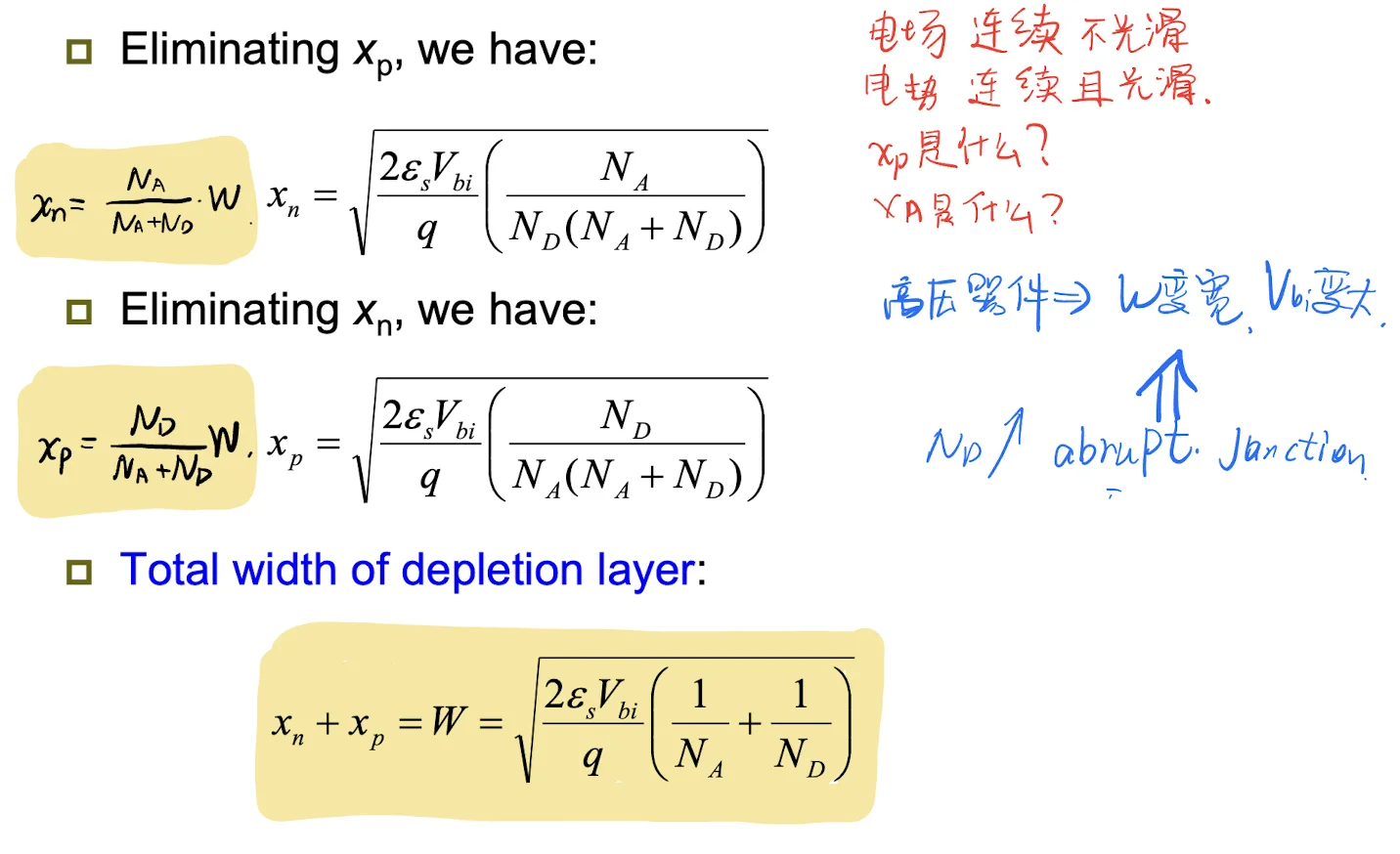
Question: 如果想要制造一个耐高压的器件(high voltage device),应该如何设计?
Answer:
To design a high-voltage abrupt PN junction, the key is to have one side heavily doped (e.g., P+) and the other side very lightly doped (e.g., an N- drift region).
This way, under reverse bias, the depletion layer (W) extends almost entirely into this lightly doped side.
A very low doping concentration (N_) allows the depletion region to become very wide, supporting a large voltage (V_) before the internal electric field reaches the critical breakdown field (E_).
要设计一个耐高压的突变PN结器件,关键是使其一侧重掺杂(例如P+),而另一侧极轻掺杂(例如N-漂移区),而不是使用“本征掺杂”。
这样,在反向偏压下,耗尽层(W)会几乎完全延伸到这个轻掺杂区。
极低的掺杂浓度 (N_) 会使耗尽层变得非常宽,从而在内部电场达到临界击穿场强(E_)之前,器件可以承受非常高的电压(V_)。
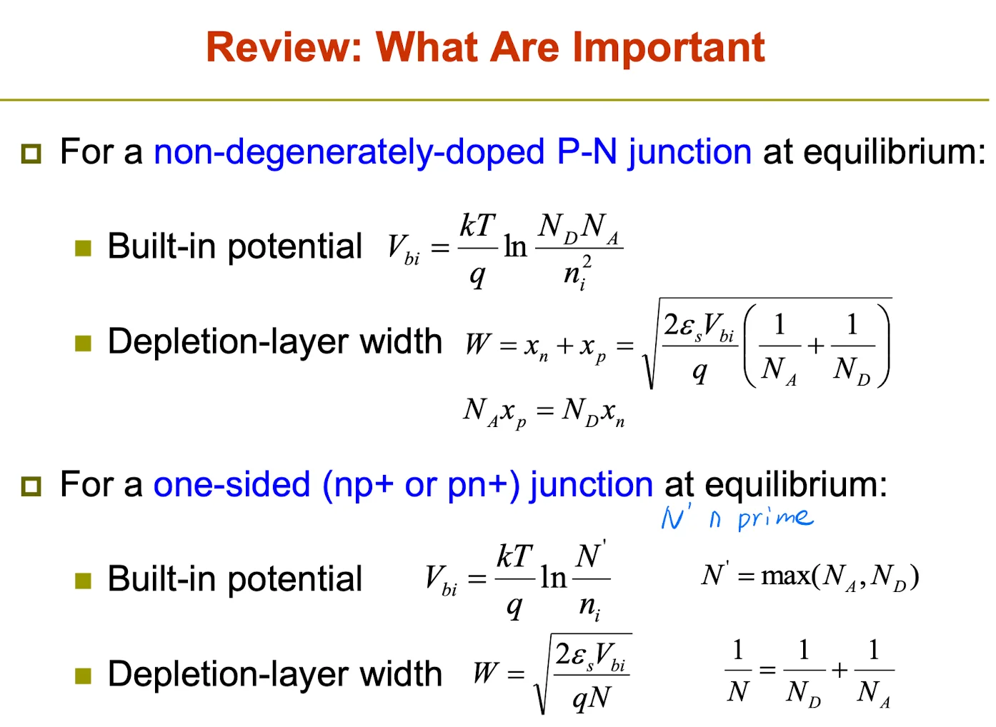
不过我觉得除非题目条件没给,不然最好不要用, 因为近似感觉不太合理
对于 而言,对于它影响的主要因素是高掺杂杂质浓度;而对于耗尽区宽度 W而言,它的主导因素是低掺杂杂质浓度
Examples | 例题
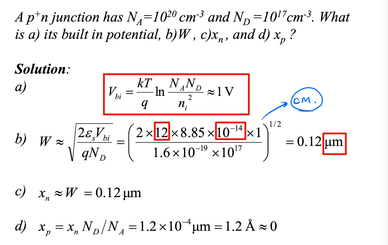
Net doping Concentration
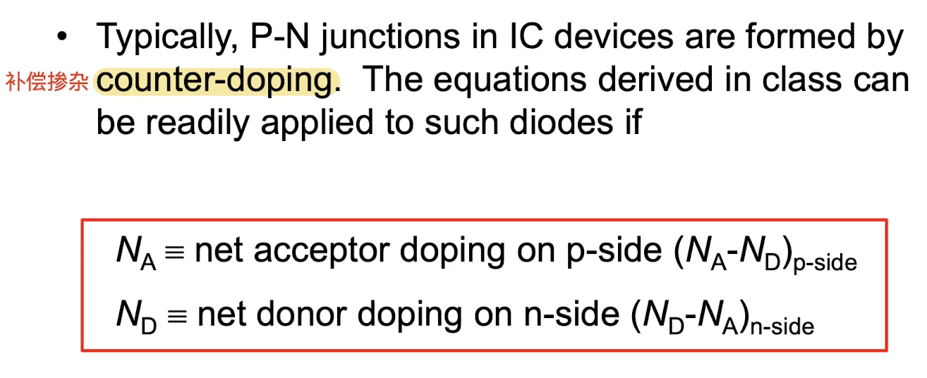
通常,集成电路(IC)器件中的P-N结是通过补偿掺杂(counter-doping)形成的
Reverse -Biased PN Junction
Question:为什么光电传感器(photo detector)一般工作在反向偏置状态?
- 反向偏置使耗尽层更宽,这增大了有效的光吸收区域,从而能产生并收集更多的光生载流子。
- 器件本身的反向偏置电流(即暗电流)非常小,因此,由光生电子-空穴对引起的额外电流变化会非常显著,易于检测。
- Reverse bias creates a wider depletion layer, which increases the effective light absorption region, thus generating and collecting more photogenerated carriers.
- The device's own reverse bias current (i.e., dark current) is very small, so the additional current change caused by photogenerated electron-hole pairs becomes very significant and easy to detect.

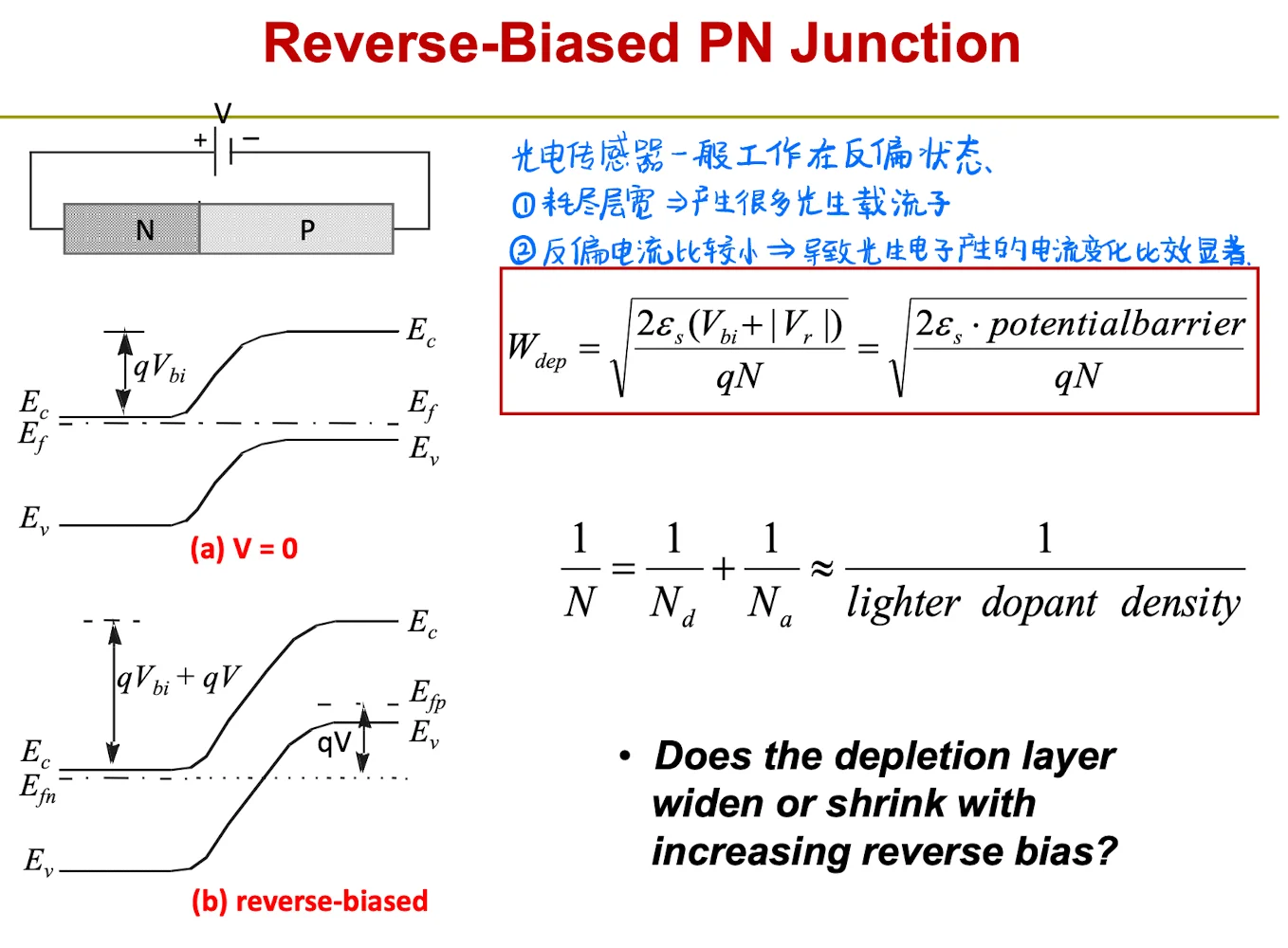
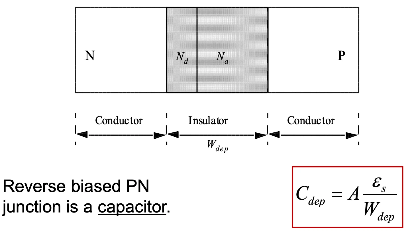
随着反向偏置电压增加,耗尽区宽度增加(widen)-> 这就导致了电容效应
Capacitance -Voltage Characteristics | 电容电压特性
Depletion Capacitance | 耗尽电容
反偏PN结(Reverse-biased Junction)的电容主要是由耗尽电容主导的
利用图像测量参数
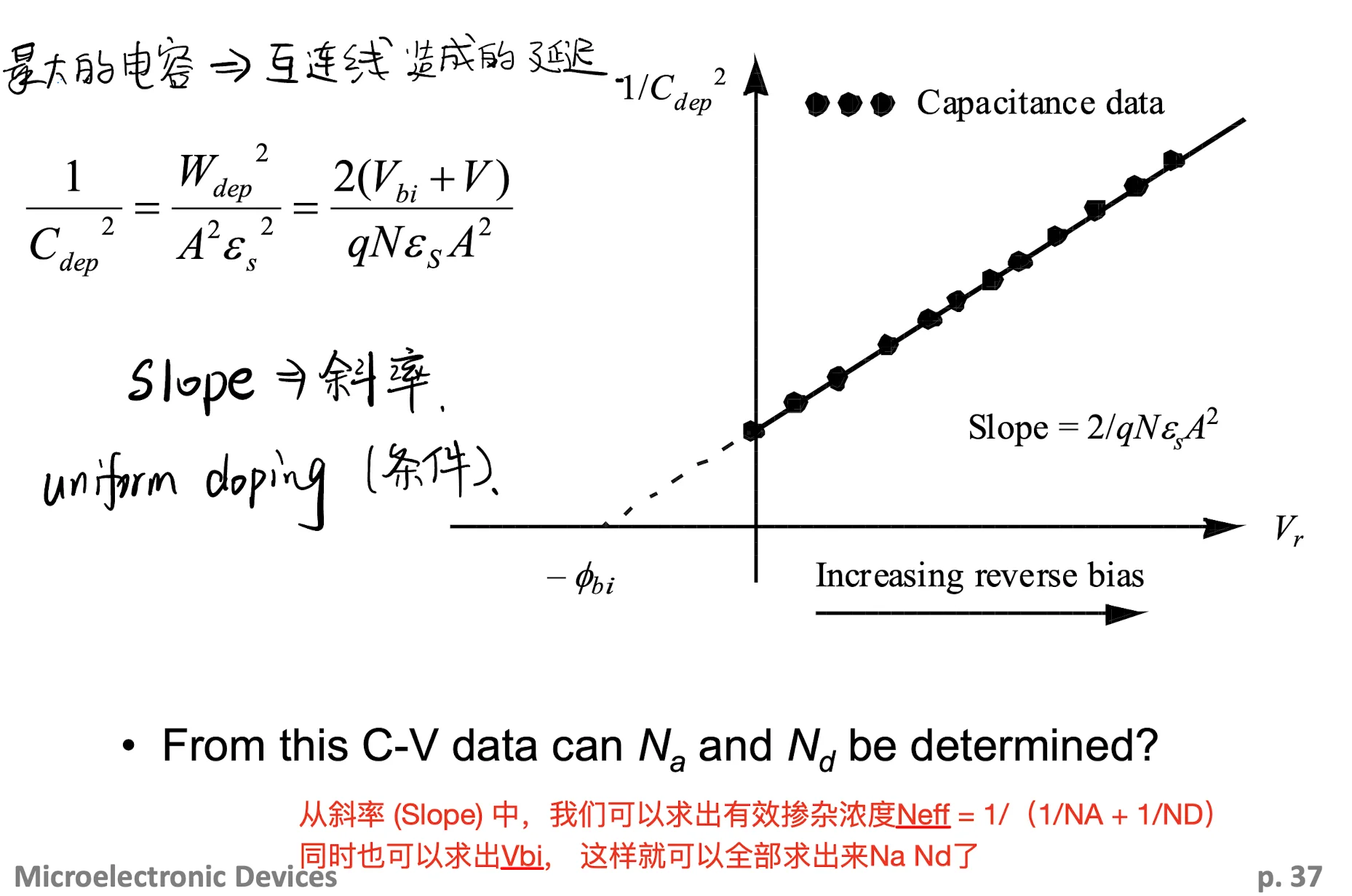
Light doping concentration approximately less than
Heavy doping concentration approximately larger than

Example | 例题
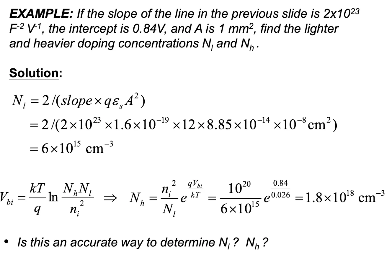
Answer:
Chinese Version
- 测量 N_l (轻掺杂): 非常准确。N_l 是根据 1/C^2 曲线的斜率 (Slope) 算出的。C-V法对轻掺杂一侧的浓度非常敏感,这是业界用于测量 N_l 的标准方法。
- 测量 N_h (重掺杂): 非常不准确。N_h 是根据截距 (V_) 反推的。由于 V_ 与 N_h 呈对数 (\ln) 关系(V_ \propto \ln(N_h)),V_ 对 N_h 的巨大变化并不敏感。反之,测量 V_ 时的微小误差,在通过指数 (e^x) 运算反推 N_h 时会被指数级放大,导致结果严重失准。
English Version
- Determining N_l (lighter doping): Very Accurate.N_l is calculated from the slope of the 1/C^2 plot. The C-V method is very sensitive to the lighter doping concentration and is the standard way to measure it.
- Determining N_h (heavier doping): Very Inaccurate. N_h is extracted from the intercept (V_). Because V_ has only a logarithmic (\ln) dependence on N_h (V_ \propto \ln(N_h)), V_ is very insensitive to large changes in N_h. Conversely, small measurement errors in V_ are exponentially (e^x) amplified when solving for N_h, leading to highly inaccurate results.
PN Junction Break Down
当给PN结施加的反向电压(V为负)大到一定程度,超过一个阈值 V_B(击穿电压)时,反向电流会突然急剧增大。这种现象就是“击穿”。
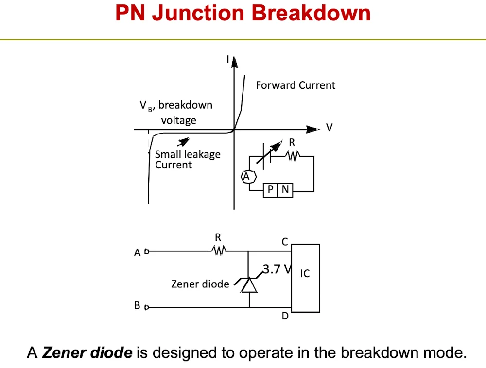
Zener Diode is designed to operate in the breakdown mode
PN结的击穿特性本身是可逆的(如果控制电流),但它导致的发热往往是不可逆的破坏。普通二极管应避免击穿;而齐纳二极管则巧妙地利用了“击穿时电压恒定”这一特性,通过特殊设计(并配合限流电阻R)使其能安全地工作在击穿区,实现了稳压功能
- 好处 (Good Thing): 击穿时,二极管两端的电压几乎恒定不变(钳位在 V_B)——Zener Diode。
- 坏处 (Bad Thing): 击穿时的大电流会产生大量的热(焦耳热),如果这个电流不加限制,高温会不可逆地 (irreversible) 烧毁器件
Breakdown Voltage
当反向电压 V_R 增大,使峰值电场 达到了材料所能承受的临界电场 E_ 时,击穿发生
|
|
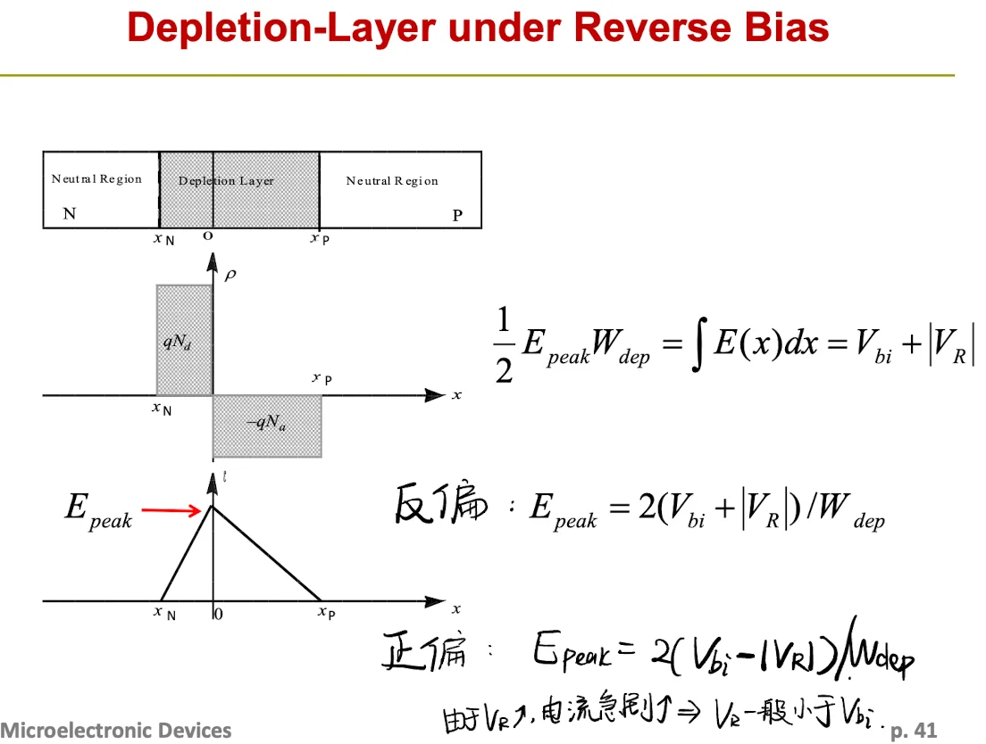
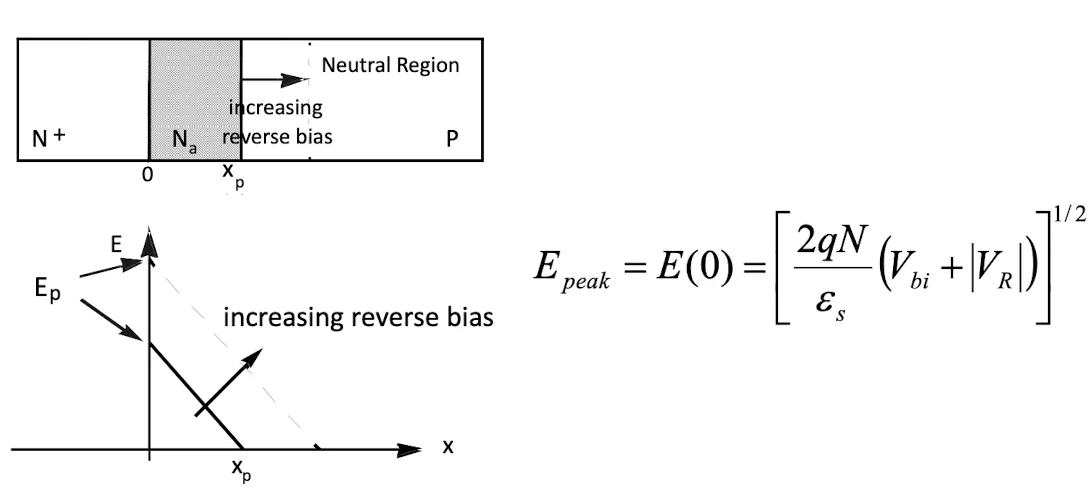
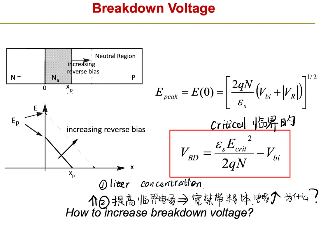
是一个材料参数(如)。
这里给出了一个重要的公式——击穿电压
如何提高击穿电压 ? (耐高压器件的设计)
- 降低掺杂浓度 ():
- 从公式 可知,掺杂越轻, V_B 越高。
- 这就是为什么高压器件需要一个宽的、极轻掺杂的“漂移区”。
- 提高临界电场 ():
- 从公式 可知, 影响巨大。
- 使用宽禁带半导体(如 SiC, GaN),它们的 远高于Si,因此是制作高压器件的理想材料。
为什么宽禁带半导体击穿场强大?
高压器件的击穿主要是雪崩击穿。这个过程依赖于碰撞电离 (Impact Ionization),碰撞电离所需要的最小动能(即“门槛能量” )正比于禁带宽度 。(一个近似值是 )
因此,逻辑链是:
宽禁带 ( 大) 碰撞电离的能量高 载流子需要被更强的电场加速,才能获得这份能量 能够触发雪崩的“临界电场” () 非常强。
Tunneling Breakdown
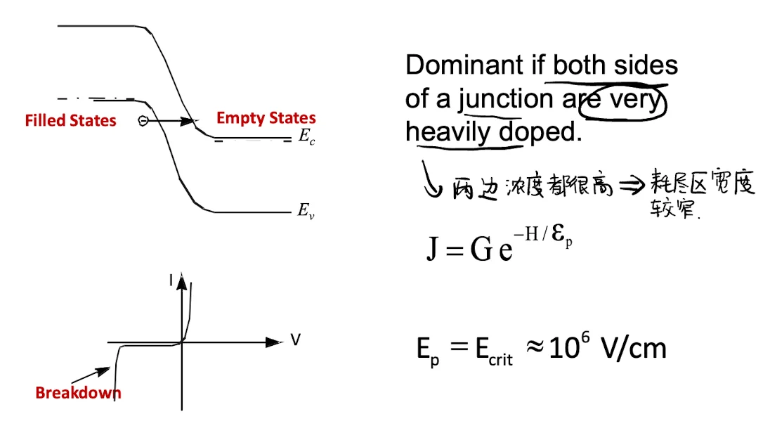
- 发生条件:
- 在两边都重掺杂 (N_A, N_D 都很高) 的PN结中占主导。
- 物理过程: 量子隧道效应 (Quantum Tunneling)
- 两边都重掺杂 耗尽区宽度非常窄( 极窄)
- 势垒虽然高,但非常薄,P区的电子(在价带)可以直接“隧穿”通过这个薄势垒,到达N区的导带,形成大电流。
- 特性:
- 通常发生在较低的电压下(例如 V_B < 5\text{V})。
- 应用: Zener Diode | 齐纳二极管
- 设计: 专门被设计用来安全工作在击穿模式的二极管。(通常 V_B < 5\text{V} 是齐纳击穿为主, V_B > 6\text{V} 是雪崩击穿为主)。
- 功能: 稳压 (Voltage Regulator) 或 电压钳位 (Clamping)。
- 电路:
- 齐纳二极管反向偏置。
- 与被保护的负载(如 IC)并联。
- 必须串联一个限流电阻 (R),以防止过热烧毁。
- 工作原理: 当输入电压(A-B)超过(例如3.7V)时,二极管击穿,将C-D两点的电压“钳位”在 (3.7V),从而保护IC。
Avalanche Breakdown | 雪崩击穿
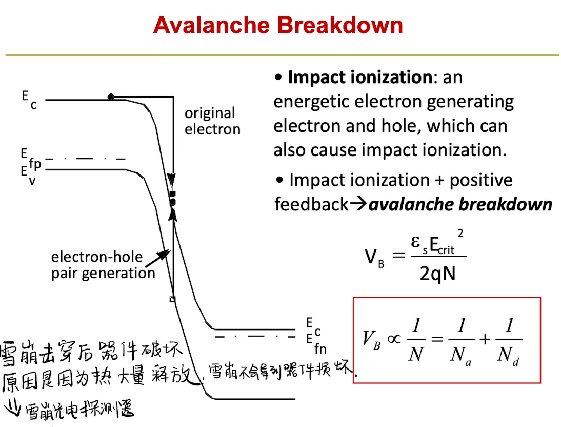
- 发生条件 | Condition:
- 在轻掺杂(或中等掺杂)的PN结中占主导。
- 此时 V_B 较高,耗尽层较宽。
- 物理过程: 碰撞电离 (Impact Ionization)
- 耗尽区电场强,电子被加速获得很高能量
高能电子撞击晶格,将价带电子“撞”出,产生一个新的电子-空穴对
新产生的载流子也被加速,再去撞击,产生更多的载流子
这个过程像雪崩一样,是一个正反馈 (Positive Feedback),导致载流子数量和电流剧增。 - In the strong electric field of the depletion region, electrons are accelerated and gain high kinetic energy.
These energetic electrons impact the crystal lattice, "knocking out" a valence electron and generating a new electron-hole pair.
The newly generated carriers are also accelerated, impacting the lattice again to generate even more carriers.
This process, like an avalanche, is a positive feedback loop, leading to a dramatic, exponential increase in carrier concentration and current.
- 耗尽区电场强,电子被加速获得很高能量
高能电子撞击晶格,将价带电子“撞”出,产生一个新的电子-空穴对
- 应用:
- 雪崩光电探测器 (APD, Avalanche Photodetector) 利用此效应来放大微弱的光信号。
- 雪崩过程本身不会损坏器件,是过热导致损坏。
评论区