What is Semiconductor | 什么是半导体
|
|
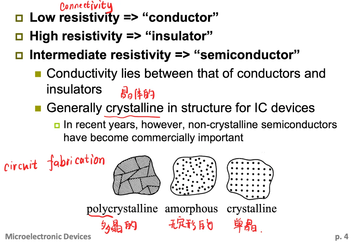
- Conductivity lies between that of conductors(导体) and insulators(绝缘体).
- Generally crystalline in structure for IC devices | 在集成电路器件中通常呈晶体结构.
- In recent years, however, non-crystalline semiconductors(非晶半导体) have become commercially important(具有商业价值)
- Graphene | 石墨烯
Typical Semiconductor |典型半导体
- Silicon: diamond cubic structure 金刚石立方结构
- GaAs: ZnS (Zinc Blende) structure
How Many Silicon Atoms per cm3?
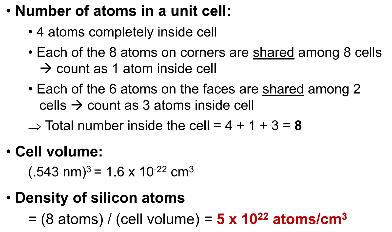
等效硅原子在一个立方晶格中是8个,每个立方晶格占地,于是可求Si 的数密度为
Compound (or elemental) Semiconductors 化合(或元素)半导体
- A compound semiconductor is a semiconducting material formed from two or more different chemical elements, like GaN.
- This is different from an elemental semiconductor, like silicon (Si), which is made from only one element.
Energy Band theory | 能带理论
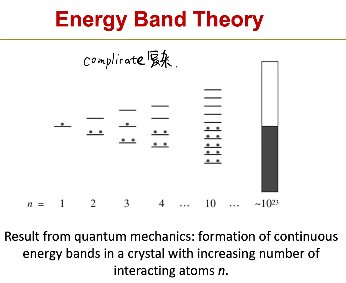
根据量子力学,在晶体中,随着相互作用原子数量 的增加,会形成连续的能带
Result from quantum mechanics: formation of continuous energy bands in a crystal with increasing number of interacting atoms
Conduction (or valence) band 导(价)带
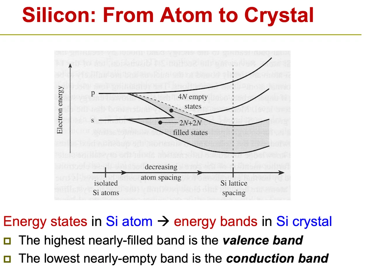
- 价带:The highest nearly-filled band is the valence band.
- 导带:The lowest nearly-empty band is the conduction band.
Energy Band Diagram | 能带图
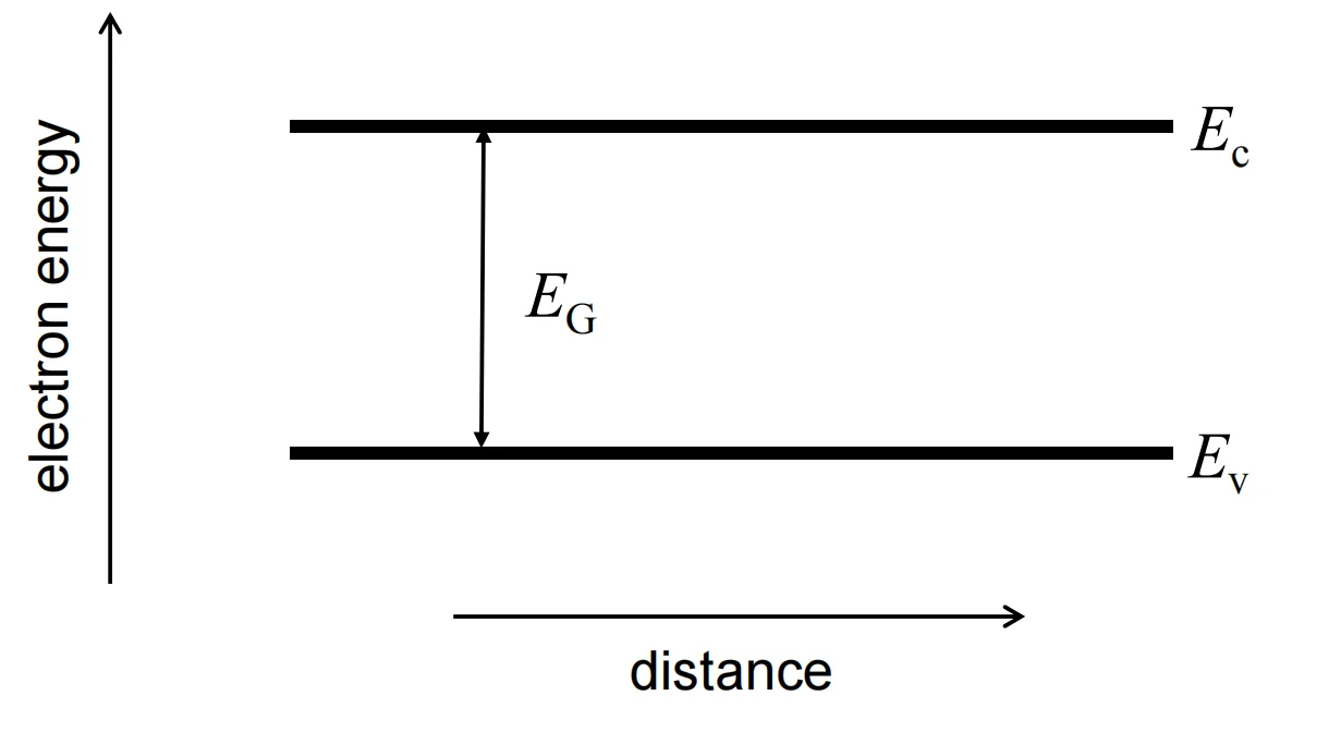
- : Bottom edge of the conduction band ()
- : Top edge of the valence band ()
and are separated by the band gap energy
Band Gap and Material Classification | 带隙与材料分类
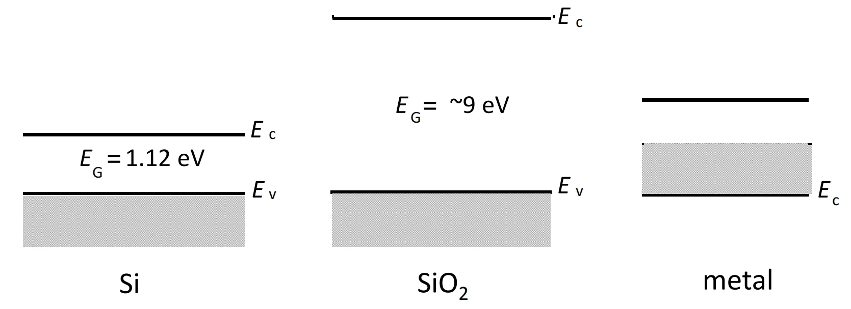
Filled bands and empty bands do not allow current flow
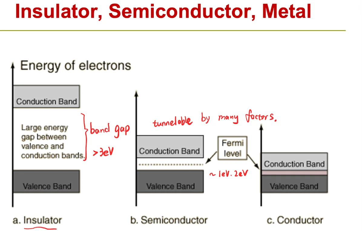
- Insulators have large | 绝缘体有很高的band gap
- Semiconductors have small | 半导体有很小的band gap
- Metals have no band gap. Conduction band is partially filled | 金属没有band gap,导带是被部分填满的
How to measure bandgap energy | 带隙测量
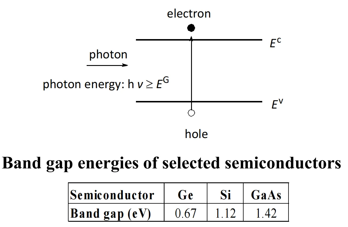
can be determined from the minimum energy of photons(光子,注意区分声子:phonon) that are absorbed by the semiconductor.
Electronic Properties of Si | 硅的电特性
- Silicon is a semiconductor material. Pure Si has high electrical resistivity at room temperature. | 纯净Si在室温有很高的电阻
- There are 2 types of mobile charge-carriers in Si:
- 电子:Conduction electrons are negatively charged;
- 空穴:Holes are positively charged.
- The concentration of conduction electrons & holes in a semiconductor can be modulated(调整) in several ways| 四种因素会影响载流子浓度:
- Adding impurity atoms (dopants) 掺杂
- Applying to an electrical field 施加电场
- Changing the temperature 改变温度
- Irradiation 辐照
Bond Model of Electrons and Holes
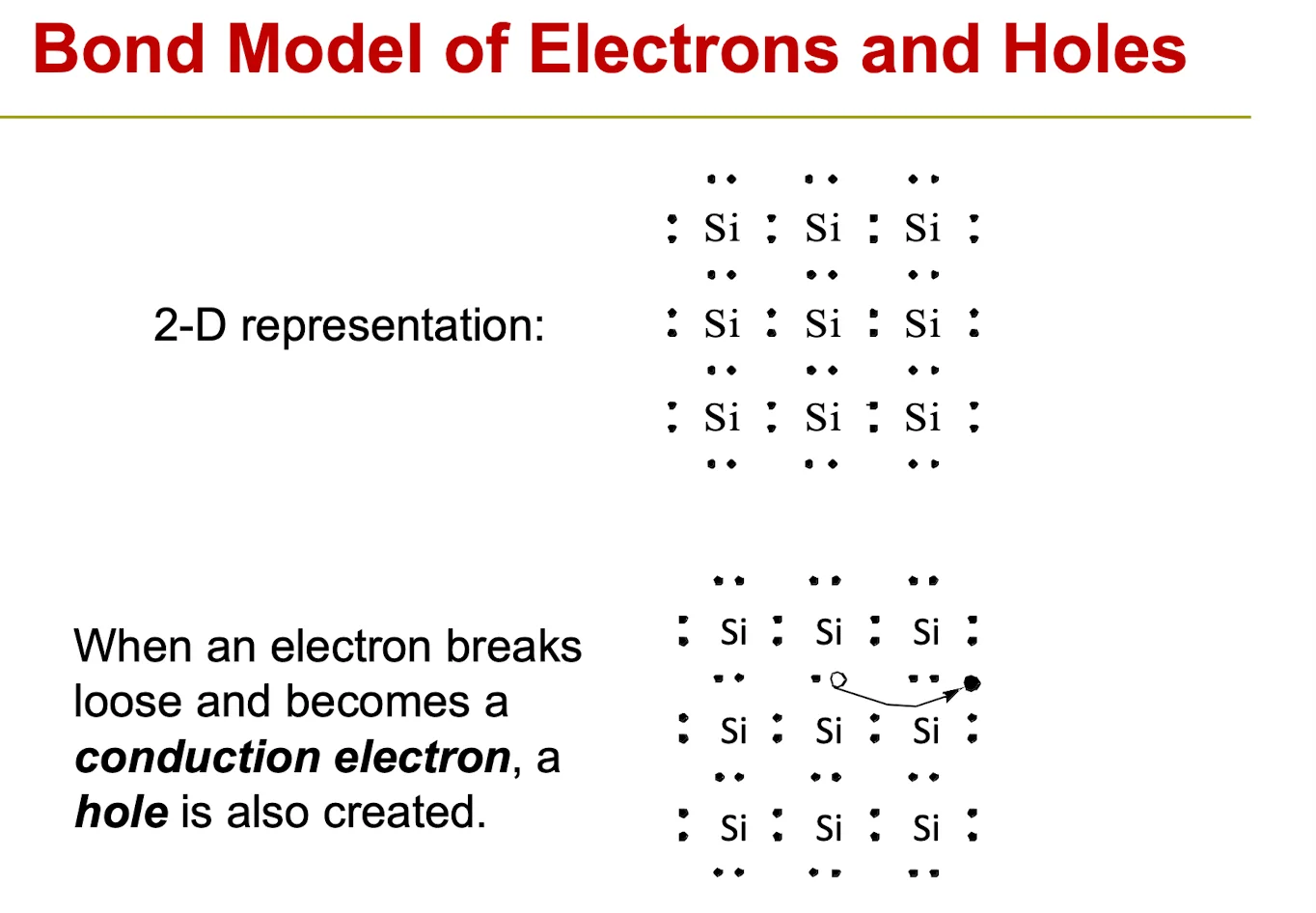
- When an electron breaks loose and becomes a conduction electron, a hole is also created.
- In a pure Si crystal, conduction electronics and holes are formed in pairs.
Hole | 空穴
Mobile positive charge associated with a half-filled covalent bond. (与半填充共价键相关的可移动正电荷)
- Treat as positively charged mobile particle(粒子) in the semiconductor.
Definition of Terms
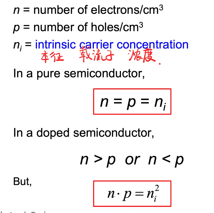
n = number of electrons/cm3
p = number of holes/cm3
= intrinsic carrier concentration
In a pure semiconductor,
In a doped semiconductor,
Bond theory: Density of state 状态密度
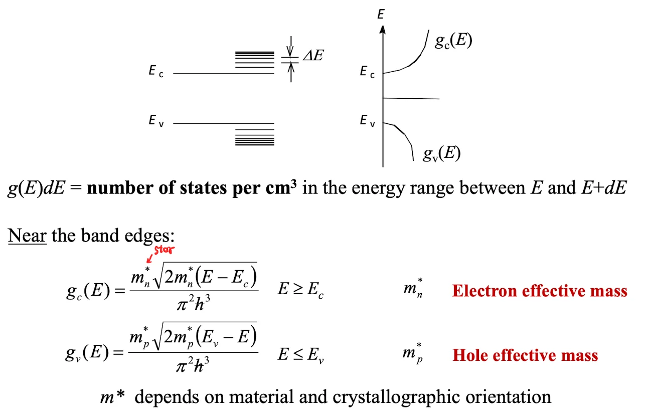
number of states per in the energy range between and
m* (effective mass) depends on material(材料) and crystallographic orientation(晶向)
Doping in Sillicon 硅掺杂

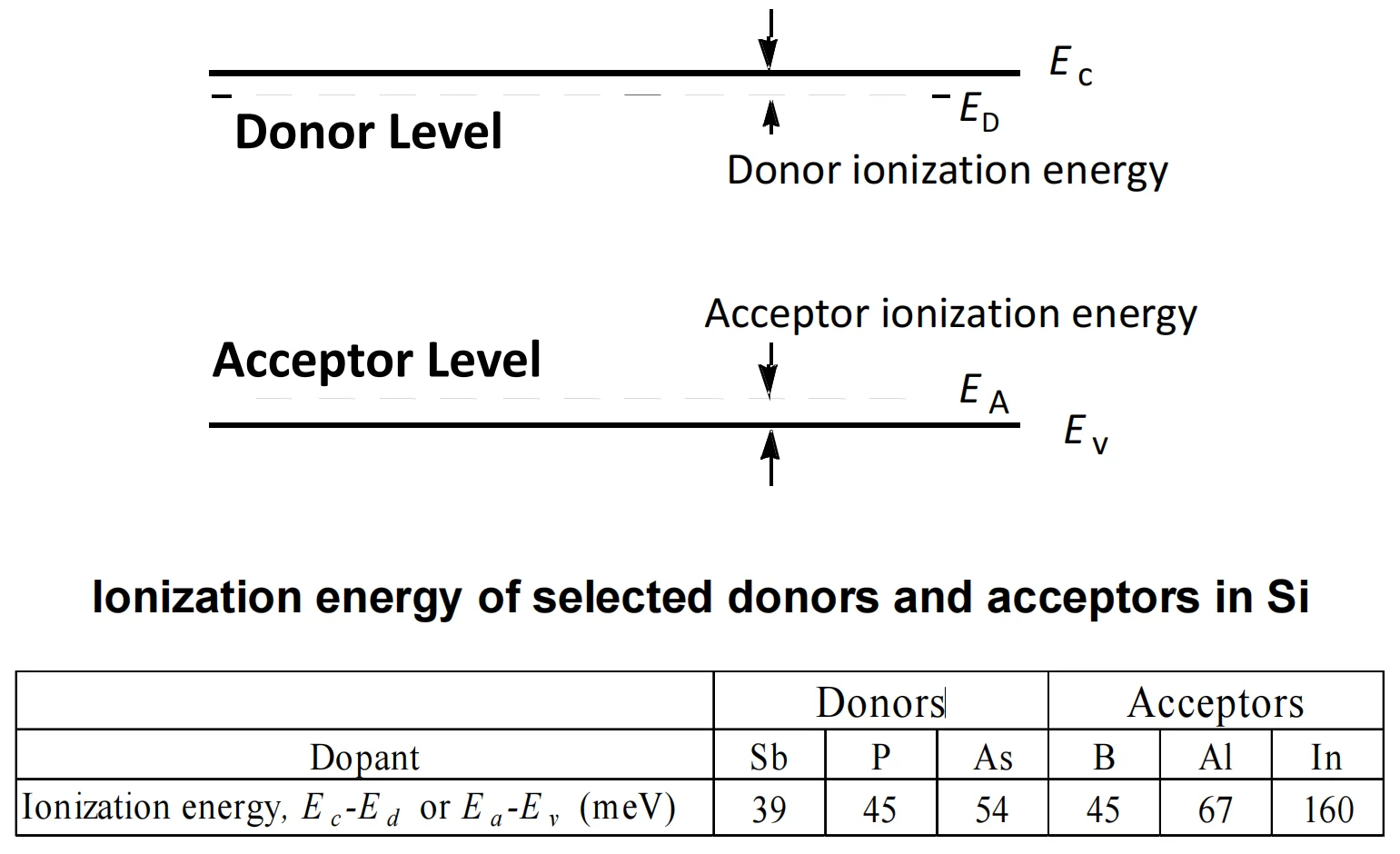
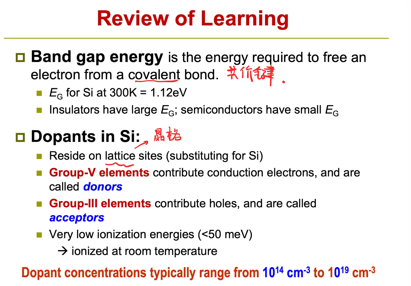
By substituting(替代) a Si atom with a special impurity atom (Group V(Donors) or Group III(Acceptors) element), a conduction electron or hole is created.
Donors: P(Phosphorus), As(Arsenic), Sb(Antimony)
Acceptors: B(Boron), Al(Aluminum), Ga(Gallium), In(Indium)
| 类型 | 元素符号 | 英文名称 |
|---|---|---|
| 施主 (Donors) | P | Phosphorus (磷) |
| As | Arsenic (砷) | |
| Sb | Antimony (锑) | |
| 受主 (Acceptors) | B | Boron (硼) |
| Al | Aluminum (铝) | |
| Ga | Gallium (镓) | |
| In | Indium (铟) |
Donor / Acceptor Levels 施主/受主能级
Charge-Carrier Concentrations | 载流子浓度
: ionized donor concentration (cm-3)
: ionized acceptor concentration (cm-3)
Charge neutrality condition:
At thermal equilibrium: (Law of Mass Action)
|
|
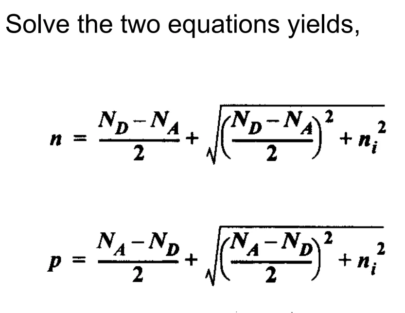
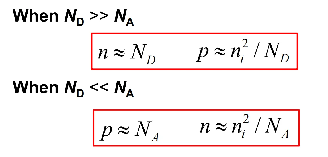
Note: Carrier concentrations depend on net dopant concentration ( - ) !
Summary
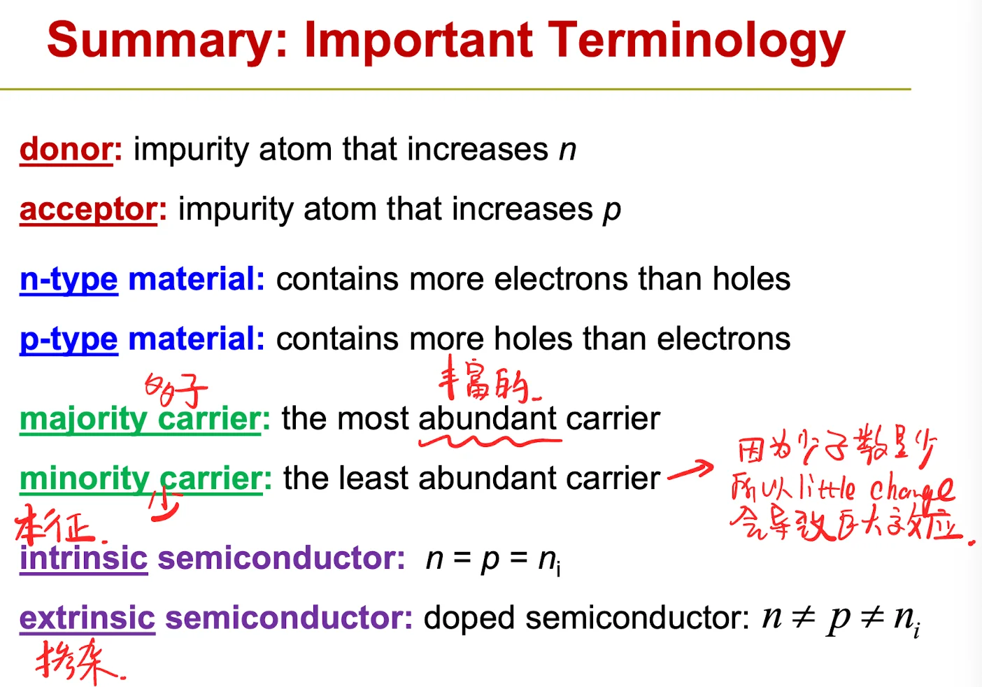
donor: impurity atom that increases n, for example Group-V elements
acceptor: impurity atom that increases p, for example Group-III elements
n-type material: contains more electrons than holes
p-type material: contains more holes than electrons
majority carrier: the most abundant carrier
minority carrier: the least abundant carrier
intrinsic semiconductor:
extrinsic semiconductor: doped semiconductor:
Dopant concentrations typically range from cm-3 to cm-3
|
|
Thermal Equilibrium | 热平衡
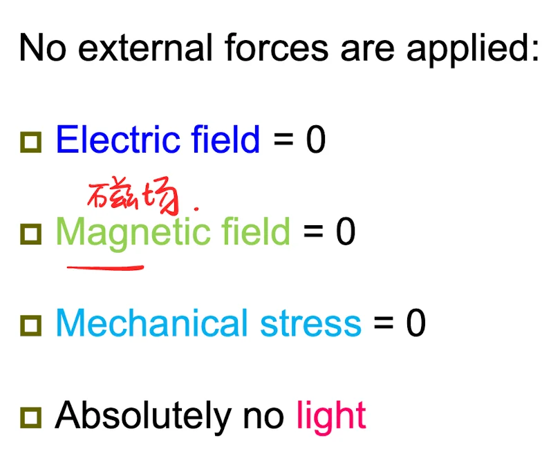
- Condition 条件:No external forces are applied:
- Electric field = 0
- Magnetic(磁) field = 0
- Mechanical stress(机械应力) = 0
- Absolutely no light
- Characteristic 特点
- Dynamic situation(动态平衡)in which every process is balanced by its inverse process.
- Electron-hole pair (EHP) generation rate = EHP recombination rate
- Thermal agitation(热运动): electrons and holes exchange energy with the crystal lattice and each other.
- Every energy state in the conduction band and valence band has a certain probability of being occupied by an electron.
- Dynamic situation(动态平衡)in which every process is balanced by its inverse process.
动态平衡状态,每个过程都与其逆过程相互平衡。
电子-空穴对(EHP)的生成速率等于其复合速率。
热运动:电子与空穴在晶体晶格中相互交换能量。
导带和价带中的每个能级都有被电子占据的概率
Fermi-Dirac Statistics 费米狄拉克统计
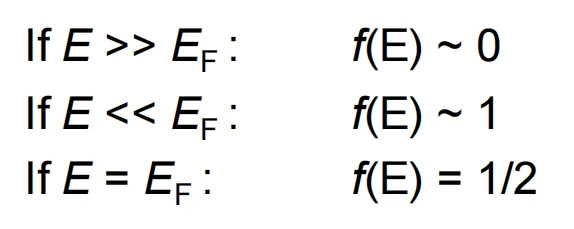
Probability that an available state at energy E is occupied is given by Fermi-Dirac distribution function:
费米狄拉克函数
There is only one Fermi level in a system at equilibrium.
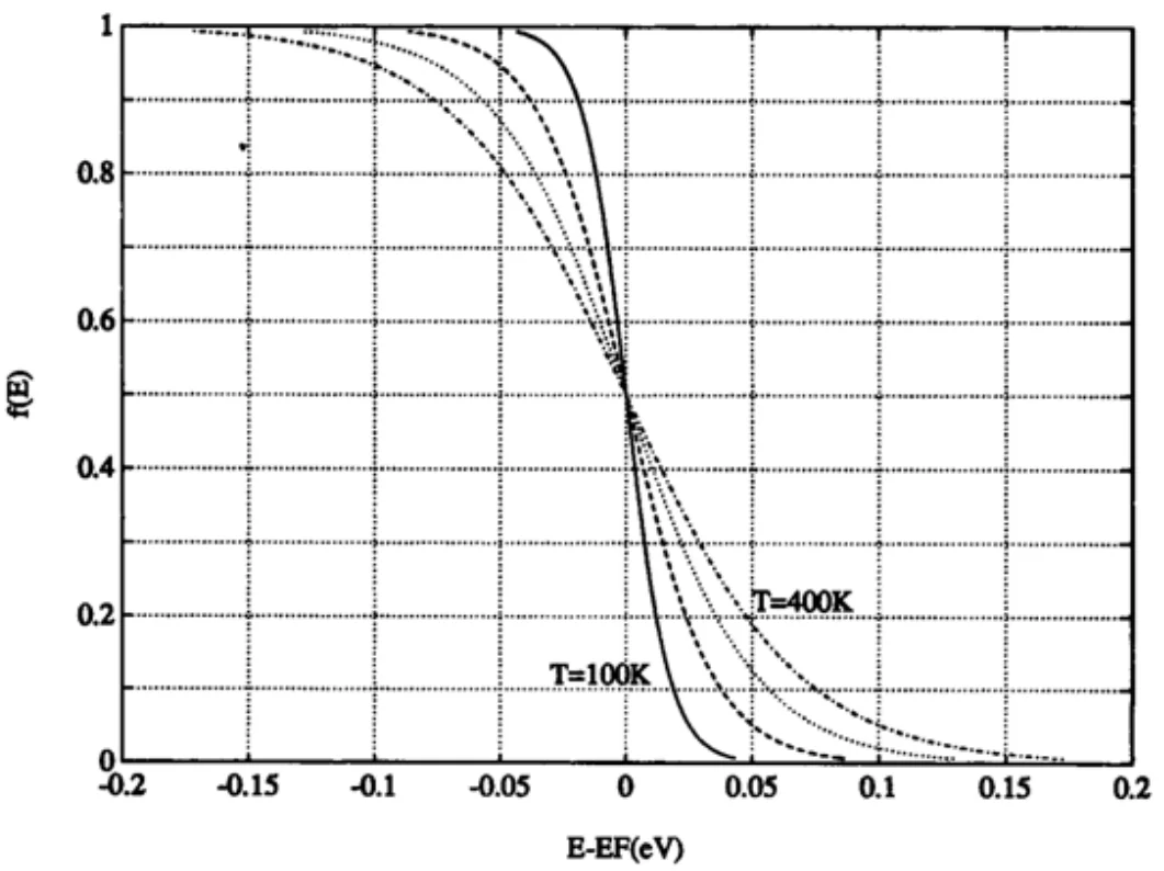
Effect of Temperature on f(E)
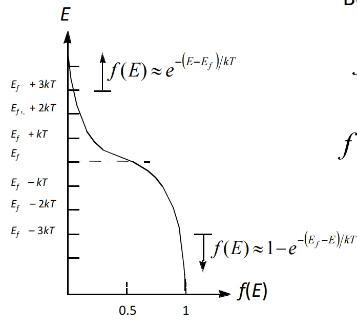
Boltzmann Approximation | 玻尔兹曼近似
Probability that a state is filled (occupied by an electron):
Probability that a state is empty (occupied by a hole):
Remember: there is only one Fermi-level in a system at equilibrium.
Distribution of Carriers (载流子分布)
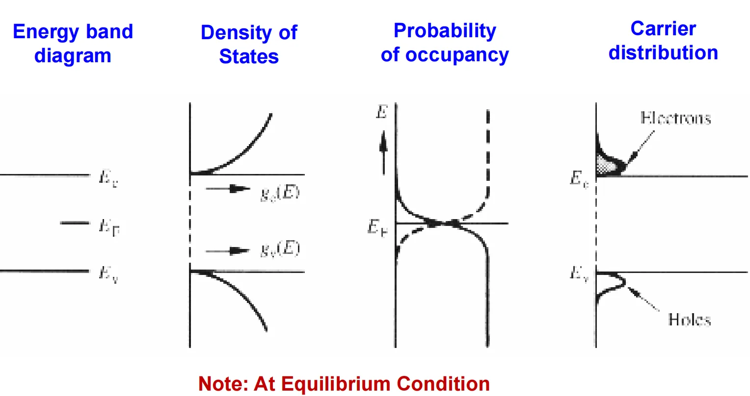
Obtain n(E) by multiplying and f(E)
Obtain p(E) by multiplying and 1-f(E)
靠近 处既有可用态 ,又有一定占据几率 ,因此电子主要分布在导带底附近
靠近 处 较大,因而空穴主要分布在价带顶附近
N-type Semiconductor Distribution (N型载流子分布)
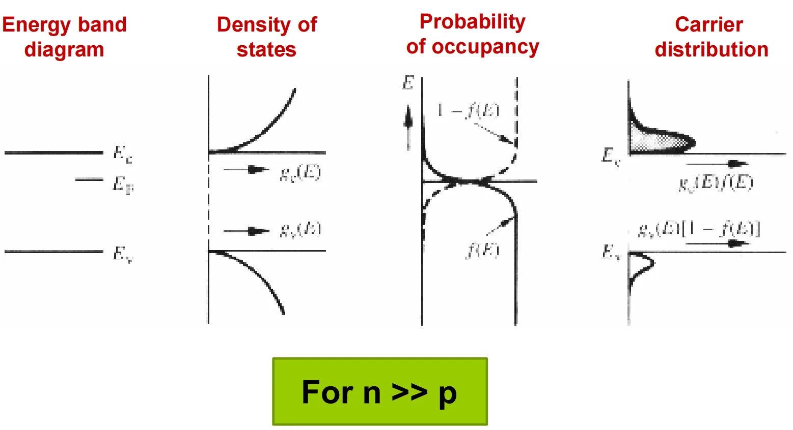
Equilibrium Electron Concentration(平衡电子浓度)
其中,Si 的 (Effective DOS of conduction band, 导带有效态密度)
P-type Semiconductor Distribution (P型载流子分布)
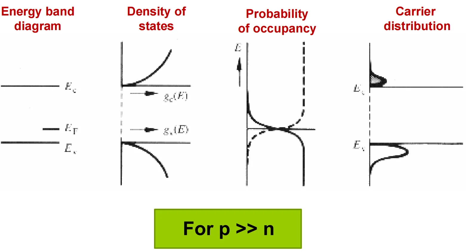
Equilibrium Hole Concentration(平衡空穴浓度)
其中,Si 的 (Effective DOS of valence band, 价带有效态密度)
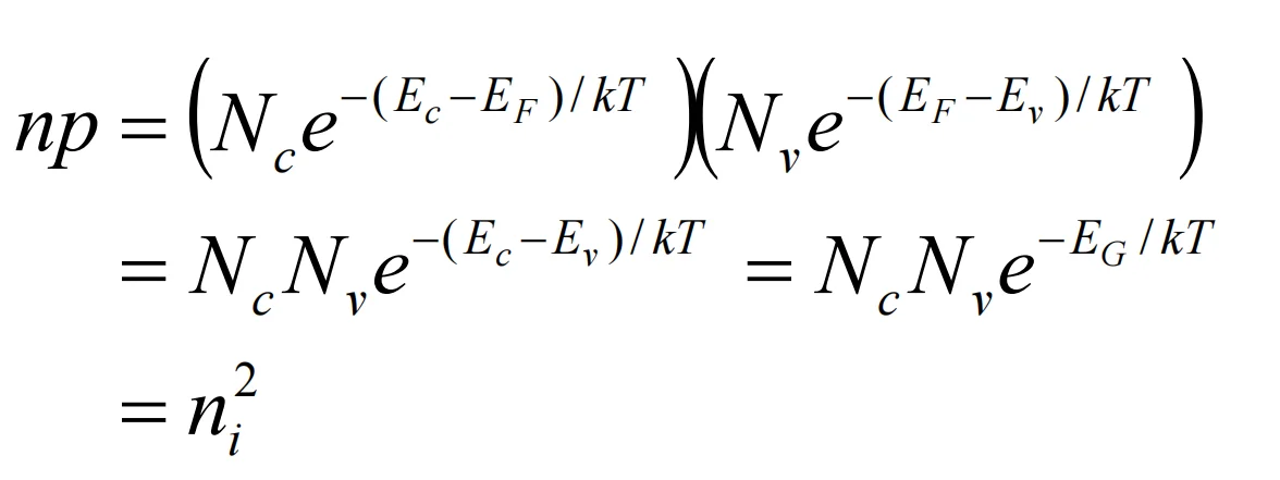
Intrinsic Carrier Concentration(本征载流子浓度)
评论区